













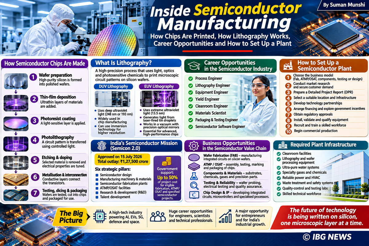

Inside the World of Semiconductor Manufacturing: How Tiny Chips Are Printed, How Lithography Works, Career Opportunities and How to Establish a Chip Manufacturing Plant
By Suman Munshi | IBG NEWS
Introduction: The Technology That Powers the Modern World
From smartphones and computers to satellites, electric vehicles, artificial intelligence, medical equipment and defence systems, almost every modern technological innovation depends on one remarkable component: the semiconductor chip.
Often smaller than a fingernail, these sophisticated electronic devices contain millions or even billions of microscopic transistors. They process information, store data, control electrical power and enable machines to communicate with one another.
But how are these tiny electronic structures actually manufactured? How can light be used to print microscopic circuits onto silicon? What is lithography, and why has it become one of the most strategically important technologies in the world?
More importantly, can young engineers build careers in this industry? Can an entrepreneur establish a semiconductor manufacturing facility in India?
The answers lie in understanding the science, engineering, economics and opportunities behind the semiconductor manufacturing ecosystem.
1. How Are Semiconductor Chips Manufactured?
Semiconductor manufacturing is an extraordinarily precise industrial process. Unlike conventional printing, where ink is transferred onto paper, chip manufacturing involves creating extremely small electronic structures on highly polished silicon wafers.
The primary raw material is high-purity silicon, a semiconductor whose electrical properties can be carefully controlled.
A typical manufacturing process involves several interconnected stages:
Step 1: Silicon wafer preparation
High-purity silicon is melted and formed into a single-crystal cylindrical ingot. The ingot is sliced into thin circular wafers, which are polished to achieve an exceptionally smooth surface.
Step 2: Thin-film deposition
Extremely thin layers of insulating, conducting or semiconductor materials are deposited on the wafer. Depending on the design, manufacturers use processes such as chemical vapour deposition (CVD), physical vapour deposition (PVD) and atomic layer deposition (ALD).
Step 3: Photoresist coating
The wafer receives a light-sensitive chemical coating known as photoresist. This material reacts to carefully controlled light exposure.
Step 4: Photolithography
A specialised machine transfers a circuit pattern from a mask or reticle onto the photoresist-coated wafer using highly controlled light.
Step 5: Development and etching
The exposed photoresist is developed to reveal the desired pattern. Chemical or plasma-based etching then removes selected portions of the underlying material.
Step 6: Ion implantation and doping
Selected regions of the silicon are modified by introducing controlled impurities. This changes their electrical characteristics and helps create the transistors and other electronic components.
Step 7: Inspection and metrology
Sophisticated optical and electronic inspection systems identify defects, measure dimensions and verify the alignment of successive layers.
Step 8: Interconnection and metallisation
Conductive structures are formed to connect the transistors into functional circuits.
Step 9: Wafer testing, dicing and packaging
The completed wafer is electrically tested and separated into individual dies. Functional dies are packaged, connected to external terminals and subjected to additional testing.
These operations are repeated many times. A modern integrated circuit may contain dozens of processing layers, with some manufacturing flows requiring hundreds of individual operations.
2. What Is Lithography? The Technology That Prints Invisible Circuits
Lithography is one of the most important technologies in semiconductor manufacturing.
The word may sound similar to conventional printing, but semiconductor lithography is fundamentally different. It uses light, precision optics, photosensitive chemicals and sophisticated positioning systems to reproduce microscopic circuit patterns on silicon wafers.
Think of it as printing an extraordinarily detailed architectural blueprint onto a surface thousands of times smaller than a sheet of paper.
The process works as follows:
- A silicon wafer is coated with photoresist.
- A reticle containing the circuit pattern is positioned inside the lithography system.
- A controlled light source illuminates the pattern.
- Precision optical components project and reduce the pattern onto the wafer.
- The photoresist undergoes a chemical change where it is exposed.
- The wafer is developed to reveal the intended pattern.
- Etching and subsequent manufacturing processes transfer the pattern into the underlying material.
The process is repeated to construct increasingly complex electronic structures.
Deep Ultraviolet (DUV) Lithography
DUV lithography uses deep ultraviolet light, commonly at wavelengths of 248 nm or 193 nm in advanced manufacturing applications.
It is widely used to manufacture semiconductor devices across a broad range of technology generations.
Advanced DUV systems can also use immersion lithography, where a liquid medium between the optical system and wafer improves resolution.
Extreme Ultraviolet (EUV) Lithography
EUV is among the most advanced technologies used to manufacture leading-edge semiconductor chips.
<escape>EUV</escape> systems operate at a wavelength of just 13.5 nanometres.
The technology generates light by firing powerful laser pulses at microscopic droplets of molten tin. The resulting light is collected and directed through specialised multilayer mirrors because conventional lenses cannot be used in the same way at this wavelength.
The entire light path operates in a vacuum because EUV radiation is absorbed by air.
The wafer stage and optical systems must maintain extraordinary precision to position and expose the circuit pattern accurately.
EUV technology is particularly important for manufacturing the most intricate layers of advanced processors.
Why Is Lithography So Important?
The performance, energy efficiency, size and manufacturing cost of semiconductor devices depend heavily on the ability to create increasingly precise structures.
Smaller and more sophisticated structures can enable higher transistor density and more advanced chip architectures. However, lithography is only one part of the equation. Materials science, deposition, etching, transistor design, interconnections and process control are equally essential.
Lithography therefore represents a combination of physics, chemistry, optics, mechanical engineering, computer science and advanced manufacturing.
3. How Does a Semiconductor Fabrication Plant Work?
A semiconductor fabrication facility, commonly called a fab, is one of the most sophisticated industrial environments in the world.
Unlike an ordinary electronics factory, a semiconductor fab requires tightly controlled environmental conditions.
Its essential infrastructure includes:
- Ultra-clean manufacturing rooms with advanced air filtration.
- Precision lithography and wafer-processing equipment.
- Ultra-pure water production and distribution systems.
- Specialised gases and high-purity chemical delivery systems.
- Advanced heating, ventilation and air-conditioning systems.
- Reliable electrical power and backup infrastructure.
- Vacuum systems and specialised exhaust treatment.
- Chemical waste treatment and environmental monitoring.
- Automated wafer transportation and manufacturing software.
- Inspection laboratories and quality-control facilities.
Even microscopic dust particles can damage a wafer or destroy a circuit pattern. Consequently, employees working inside cleanrooms wear specialised protective garments.
Production is also highly automated. Computer-controlled equipment transports wafers between processing stations while manufacturing execution systems track every operation.
The entire production process requires close coordination between engineers, equipment manufacturers, chemical suppliers, software specialists and quality-control teams.

